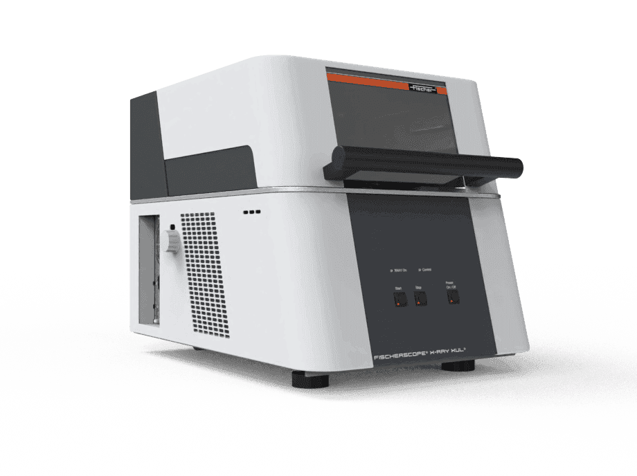

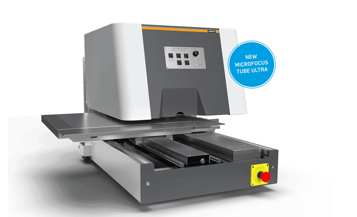

FISCHERSCOPE® X-RAY XDV®-µ PCB
The professional series for PCBs.
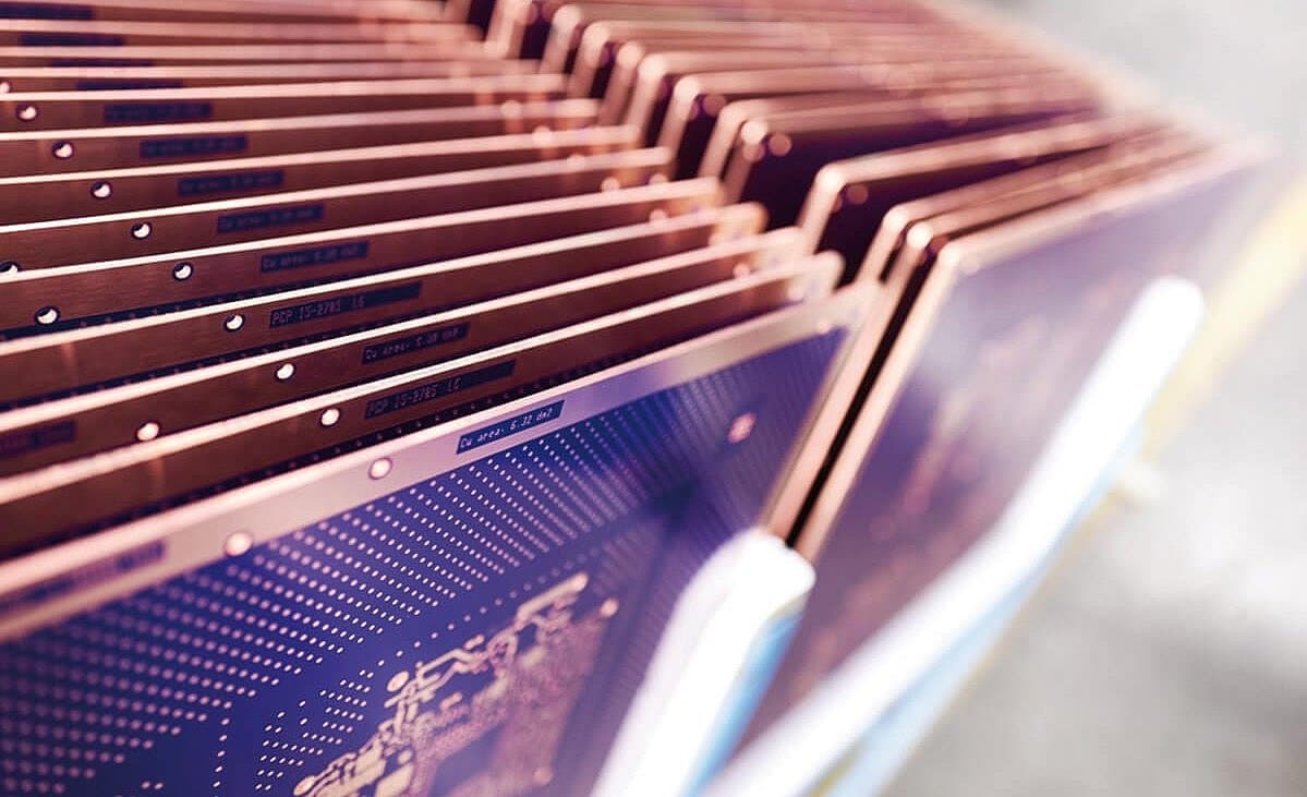
Reliable and fully automatic! The XDV® µ-PCB devices are the specialized solution for measuring smallest structures as well as very thin coatings on PCBs.
Key Benefits
- Meeting all challenges.: Reliable and fast results for ambitious measuring tasks
- Fully automatable.: Let your instrument work for you
- PCB experts.: Specialized measuring solutions for printed circuit boards, fulfill IPC standards
- Most advanced polycapillary optics on the market.: Our in-house manufactured polycapillary optics deliver outstanding measurement results in short measuring times
Description
Reliable and fully automatic! The XDV®-µ PCB devices are the specialized solution for measuring smallest structures as well as very thin coatings on PCBs.
¹ Up to 50 % increased performance: Significantly improved standard deviation and thus gauge capability or significantly reduced measurement time compared DPP to DPP+. ² High-end capillary optics made by Fischer – the world's only manufacturer of X-ray fluorescence measuring instruments with its own polycapillary production. Three different high-end polycapillaries available – the right solution for each of your applications: 10 µm halo-free, 20 µm halo-free or 20 µm halo.
The FISCHERSCOPE® X-RAY XDV®-µ PCB is a true specialist for reliable quality control of PCBs with X-ray fluorescence. Thanks to a powerful silicon drift detector, microfocus tube Ultra and polycapillary optics, the XRF instrument measures with an extremely small measuring spot at very high intensity. This allows you to reliably determine even the thinnest layers. The devices also meet IPC requirements 4552 and 4556 for ENIG and ENEPIG as well as 4553A (Silver) and 4554 (Tin).
Reliable and fast results for ambitious measuring tasks
Let your instrument work for you
Specialized measuring solutions for printed circuit boards, fulfill IPC standards
Our in-house manufactured polycapillary optics deliver outstanding measurement results in short measuring times
Automated measurements on predefined structures thanks to advanced pattern recognition technology
Extremely fast and simple
Shorter measuring times or improvement of standard deviation*
*compared to the DPP
Microfocus tube Ultra with tungsten anode for even higher performance on smallest spots; Molybdenum anode optional
4-fold changeable filters
Up to 10 mm possible height of samples
Polycapillary optics allow particularly small measuring spots with short measuring times at high intensity
Measuring spot approx.: Ø 10 or 20 µm (FWHM)
High-precision, programmable measuring table for PCBs up to 610 x 610 mm, optionally with vacuum fixture
Silicon drift detector with 20 or 50 mm² for highest precision on thin films
DPP+ for highest precision even with short measuring times
Do you have further applications? Then contact us!
Features
- Microfocus tube Ultra with tungsten anode for even higher performance on smallest spots; Molybdenum anode optional
- 4-fold changeable filters
- Up to 10 mm possible height of samples
- Polycapillary optics allow particularly small measuring spots with short measuring times at high intensity
- Measuring spot approx.: Ø 10 or 20 µm (FWHM)
- High-precision, programmable measuring table for PCBs up to 610 x 610 mm, optionally with vacuum fixture
- Silicon drift detector with 20 or 50 mm² for highest precision on thin films
- DPP+ for highest precision even with short measuring times
- Fischer DPP+ ¹ for highest precision even with short measuring times
- Polycapillary optics produced in-house² with smallest spot size 10 µm (FWHM)
- Automatic image recognition for reliable measuring of small structures
- Measuring on smallest flat components and structures on PCBs up to 610 x 610 mm (24 x 24 in)
- Analysis of very thin coatings, such as gold/palladium layers of ≤ 3 nm or 10 nm
- Automated measuring such as in quality control
- With the 10 μm option: Measuring with smallest measuring spot in combination with a large silicon drift detector
- With the vacuum table option: Measuring on flexible PCBs
- Full compliance with IPC standards 4552 and 4556 (ENIG, ENEPIG), 4553A (Silver) and 4554 (Tin)
Documents
- AN050 X-ray instruments for standard PCB applications0.72 MB
- AN072 Simplifying quality control on PCBs with automatic pattern recognition0.67 MB
- AN088 Fast and non-destructive nickel phosphorus analysis for printed circuit boards2.40 MB
- AN092 How to choose an XRF instrument1.29 MB
- AN105 μ-spot measurements of tin and tin alloy coatings on PCBs0.82 MB
- Product overview: Complete portfolio3.17 MB
- Product overview: FISCHERSCOPE® X-RAY series3.67 MB