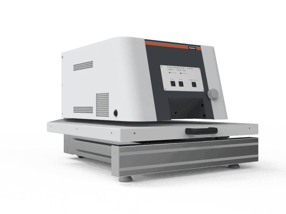

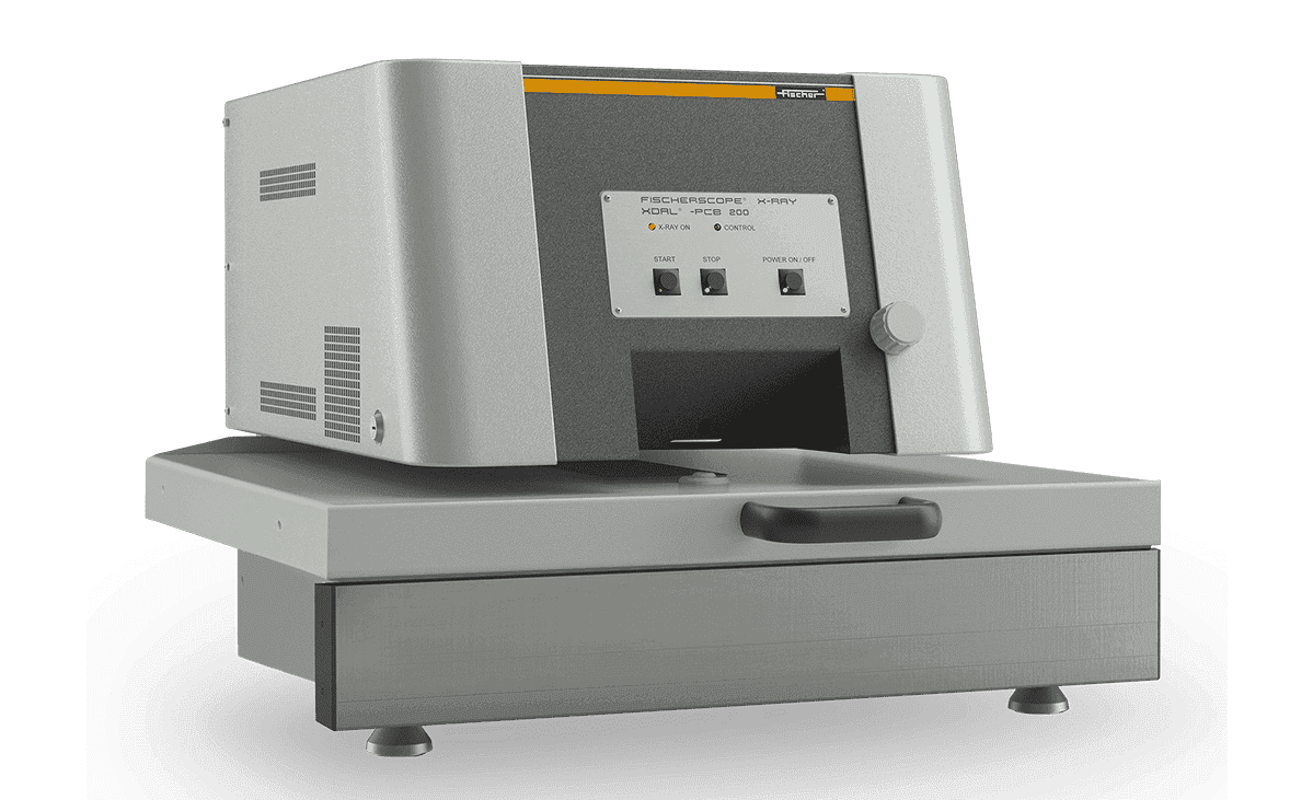
FISCHERSCOPE® X-RAY XDAL®-PCB
The high-end all-rounder.
Universal instrument for measurements on small structures, multilayer coatings, functional coatings and thin coatings < 0.1 µm.
Key Benefits
- PCB experts.: Specialized measuring solutions for printed circuit boards, fulfill IPC standards
- Meeting all challenges.: Reliable and fast results for ambitious measuring tasks
- Fully automatable.: Let your instrument work for you
- Programmable.: Automated measurements on predefined structures thanks to advanced pattern recognition technology
Description
Universal instrument for measurements on small structures, multilayer coatings, functional coatings and thin coatings < 0.1 µm.
The combination of a powerful silicon drift detector, multi-aperture and changeable filters makes FISCHERSCOPE® X-RAY XDAL®-PCB instruments predestined for measuring small structures on PCBs.
Specialized measuring solutions for printed circuit boards, fulfill IPC standards
Reliable and fast results for ambitious measuring tasks
Let your instrument work for you
Automated measurements on predefined structures thanks to advanced pattern recognition technology
Extremely fast and simple
Microfocus tube with tungsten anode
Fixed, wide measuring table for PCBs up to 610 × 610 mm, optionally with measuring table extension 1200 x 900 mm or in automated version, depending on device
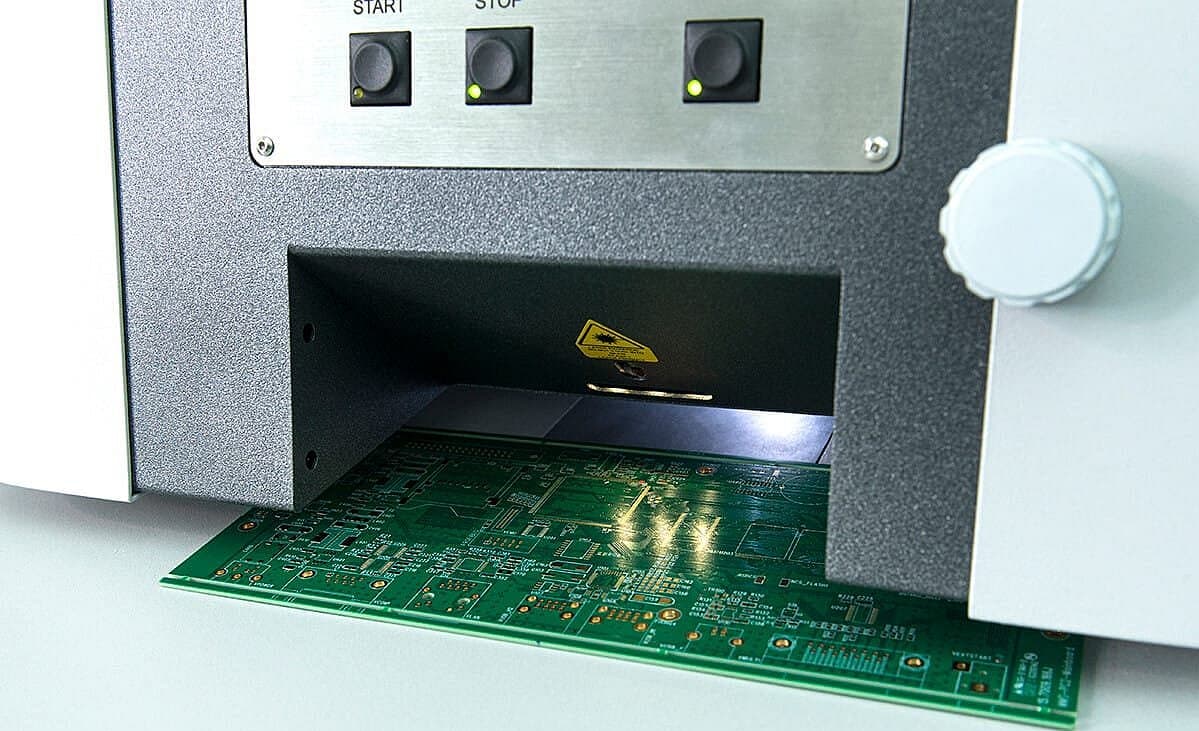
Measuring spot approx.: Ø 0.2 mm
4-fold changeable apertures and 3-fold changeable filters
Up to 10 mm possible height of samples
Large silicon drift detector for highest precision on thin layers
Do you have further applications? Then contact us!
Features
- Microfocus tube with tungsten anode
- Fixed, wide measuring table for PCBs up to 610 × 610 mm, optionally with measuring table extension 1200 x 900 mm or in automated version, depending on device
- Measuring spot approx.: Ø 0.2 mm
- 4-fold changeable apertures and 3-fold changeable filters
- Up to 10 mm possible height of samples
- Large silicon drift detector for highest precision on thin layers
- Smallest measuring spot approx. Ø 0.2 µm
- 4-fold changeable apertures 3-fold changeable filters
- Large Silicon drift detector for very good detection accuracy and high resolution
- Measuring on smallest components and structures on PCBs up to 610 x 610 mm (24 x 24 in)
- Measuring functional coatings in the electronics and semiconductor industry
- Analysis of very thin coatings of ≤ 0.1 μm
- Determination of lead content in solders
- Determination of complex multilayer systems
- Direct phosphorus determination of NiP coatings
- Meets ENIG/ENEPIG requirements
Documents
- AN050 X-ray instruments for standard PCB applications0.72 MB
- AN072 Simplifying quality control on PCBs with automatic pattern recognition0.67 MB
- AN092 How to choose an XRF instrument1.29 MB
- AN096 Optimized for the PCB industry: Measure ultrathin layers of gold and palladium according to IPC-4552B/IPC-4556A0.76 MB
- Product overview: Complete portfolio3.17 MB
- Product overview: FISCHERSCOPE® X-RAY series3.67 MB